PHYSICS / ENGINEERING / COMPUTING
Microelectronics models
Derive carrier, junction, transistor, small-signal, and noise models with twenty numerical device and circuit examples.
Matter pathway: atom → solid → liquid → gas → plasma. Quantum mechanics and quantum field theory provide foundations across the pathway; they are not additional phases. This is a connected modeling route, not a universal heating curve. Actual phases depend on pressure, composition, and kinetics.
1. Carrier statistics and conduction
Definitions & inputs. n,p are electron/hole densities, ni intrinsic density, μn,μp mobilities; q=1.602176634×10⁻¹⁹ C.
Equilibrium mass action relates carrier populations.
Add electron and hole conductivity, then apply uniform-bar geometry.
Thermal voltage sets diffusion and diode voltage scales.
Interpretation. Mobility and intrinsic density depend strongly on material and temperature.
↑ Return to definitions and contents2. Junction electrostatics and current
Definitions & inputs. NA,ND are acceptor/donor densities; εs permittivity; VR positive reverse bias; IS saturation current; η ideality factor.
Fermi-level alignment creates a built-in potential.
Integrate Poisson’s equation in depleted regions and enforce charge neutrality.
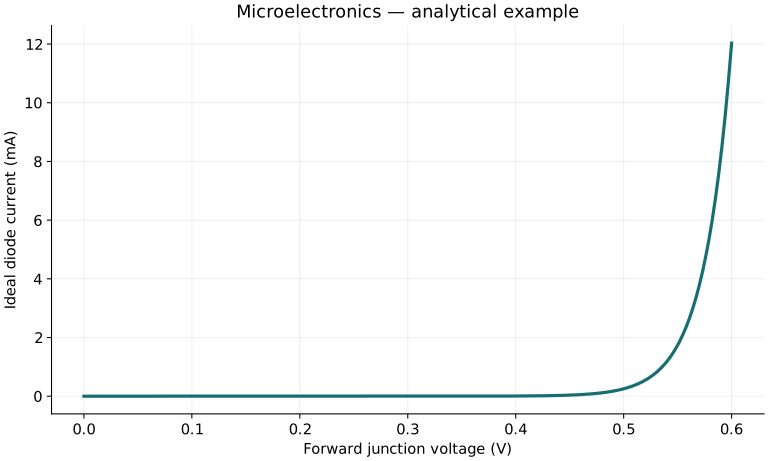
Diffusion current is exponential; differentiation yields incremental resistance well above leakage.
Interpretation. Breakdown, tunneling, parasitics, and heating are outside this diode law.
↑ Return to definitions and contents3. Long-channel MOS and small-signal gain
Definitions & inputs. Cox is oxide capacitance per area, β=μCoxW/L, Vov=VGS−Vth, λ channel-length-modulation coefficient.
Gate electrostatics set the local inversion charge.
Integrate drift current along the channel before pinch-off.
At VDS≥Vov use saturation, then differentiate at the bias point.
Interpretation. Bias conditions must be checked before selecting a region equation.
↑ Return to definitions and contents4. Time response, sampling, and noise
Definitions & inputs. R,C are lumped resistance/capacitance; B bandwidth; T absolute temperature.
Kirchhoff’s law gives a first-order charge response.
Thermal resistor noise and sampled capacitor noise have different circuit interpretations.
The first-order low-pass magnitude falls by 3 dB at this frequency.
Interpretation. Noise bandwidth may differ from a circuit’s −3 dB bandwidth.
↑ Return to definitions and contentsGraphical worked example
Twenty worked examples
Open a problem to see its defined inputs, assumptions, equation, numerical substitution, result, and interpretation. Values are illustrative analytical exercises.
Example 01. Thermal voltage
Definitions & inputs. T=300 K, kB=1.380649×10⁻²³ J/K.
Choose the governing model and isolate the requested quantity.
Insert the stated inputs in consistent units or the explicitly defined normalized units.
Evaluate the expression; the result uses the units shown.
Interpretation. About 25.85 mV sets a common room-temperature scale.
↑ Return to definitions and contentsExample 02. Minority carriers
Definitions & inputs. n=10²² m⁻³, ni=10¹⁶ m⁻³.
Choose the governing model and isolate the requested quantity.
Insert the stated inputs in consistent units or the explicitly defined normalized units.
Evaluate the expression; the result uses the units shown.
Interpretation. Majority doping suppresses equilibrium minority density.
↑ Return to definitions and contentsExample 03. Electron conductivity
Definitions & inputs. n=10²² m⁻³, μn=0.1 m²/(V s), hole contribution negligible.
Choose the governing model and isolate the requested quantity.
Insert the stated inputs in consistent units or the explicitly defined normalized units.
Evaluate the expression; the result uses the units shown.
Interpretation. Mobility is a stated model input.
↑ Return to definitions and contentsExample 04. Resistor geometry
Definitions & inputs. Resistivity ρ=10⁻⁴ Ωm, length 10 µm, cross section 1 µm².
Choose the governing model and isolate the requested quantity.
Insert the stated inputs in consistent units or the explicitly defined normalized units.
Evaluate the expression; the result uses the units shown.
Interpretation. Aspect ratio controls resistance for fixed material.
↑ Return to definitions and contentsExample 05. Built-in voltage
Definitions & inputs. VT=0.02585 V, NA=ND=10²³ m⁻³, ni=10¹⁶ m⁻³.
Choose the governing model and isolate the requested quantity.
Insert the stated inputs in consistent units or the explicitly defined normalized units.
Evaluate the expression; the result uses the units shown.
Interpretation. This internal equilibrium potential is not an externally extractable battery voltage.
↑ Return to definitions and contentsExample 06. Depletion width
Definitions & inputs. εs=1.04×10⁻¹⁰ F/m, NA=ND=10²² m⁻³, Vbi+VR=1 V.
Choose the governing model and isolate the requested quantity.
Insert the stated inputs in consistent units or the explicitly defined normalized units.
Evaluate the expression; the result uses the units shown.
Interpretation. The result includes both depleted sides.
↑ Return to definitions and contentsExample 07. Forward diode current
Definitions & inputs. IS=1 pA, V=0.5 V, η=1, VT=0.02585 V.
Choose the governing model and isolate the requested quantity.
Insert the stated inputs in consistent units or the explicitly defined normalized units.
Evaluate the expression; the result uses the units shown.
Interpretation. Series resistance can limit actual current at larger forward bias.
↑ Return to definitions and contentsExample 08. Diode incremental resistance
Definitions & inputs. I=1 mA, η=1, VT=25.85 mV.
Choose the governing model and isolate the requested quantity.
Insert the stated inputs in consistent units or the explicitly defined normalized units.
Evaluate the expression; the result uses the units shown.
Interpretation. This is local slope resistance, not V/I.
↑ Return to definitions and contentsExample 09. Oxide capacitance density
Definitions & inputs. εox=3.45×10⁻¹¹ F/m; tox=10 nm.
Choose the governing model and isolate the requested quantity.
Insert the stated inputs in consistent units or the explicitly defined normalized units.
Evaluate the expression; the result uses the units shown.
Interpretation. Thinner ideal dielectric increases capacitance density.
↑ Return to definitions and contentsExample 10. Gate capacitance
Definitions & inputs. Cox=0.00345 F/m²; gate area 1 µm².
Choose the governing model and isolate the requested quantity.
Insert the stated inputs in consistent units or the explicitly defined normalized units.
Evaluate the expression; the result uses the units shown.
Interpretation. Fringing and overlap would add capacitance.
↑ Return to definitions and contentsExample 11. MOS saturation current
Definitions & inputs. β=1 mA/V²; Vov=0.2 V.
Choose the governing model and isolate the requested quantity.
Insert the stated inputs in consistent units or the explicitly defined normalized units.
Evaluate the expression; the result uses the units shown.
Interpretation. Check VDS≥0.2 V before using this result.
↑ Return to definitions and contentsExample 12. MOS triode current
Definitions & inputs. β=1 mA/V²; Vov=0.2 V; VDS=0.05 V.
Choose the governing model and isolate the requested quantity.
Insert the stated inputs in consistent units or the explicitly defined normalized units.
Evaluate the expression; the result uses the units shown.
Interpretation. VDS<Vov places the device in this model’s triode region.
↑ Return to definitions and contentsExample 13. Transconductance
Definitions & inputs. ID=20 µA; Vov=0.2 V.
Choose the governing model and isolate the requested quantity.
Insert the stated inputs in consistent units or the explicitly defined normalized units.
Evaluate the expression; the result uses the units shown.
Interpretation. An incremental gate voltage modulates drain current through gm.
↑ Return to definitions and contentsExample 14. Output resistance
Definitions & inputs. λ=0.1 V⁻¹; ID=20 µA.
Choose the governing model and isolate the requested quantity.
Insert the stated inputs in consistent units or the explicitly defined normalized units.
Evaluate the expression; the result uses the units shown.
Interpretation. Channel-length modulation makes saturation current voltage-dependent.
↑ Return to definitions and contentsExample 15. Common-source gain
Definitions & inputs. gm=0.2 mS; RD=10 kΩ; ro≫RD.
Choose the governing model and isolate the requested quantity.
Insert the stated inputs in consistent units or the explicitly defined normalized units.
Evaluate the expression; the result uses the units shown.
Interpretation. The negative sign indicates inversion.
↑ Return to definitions and contentsExample 16. RC time constant
Definitions & inputs. R=10 kΩ, C=10 pF.
Choose the governing model and isolate the requested quantity.
Insert the stated inputs in consistent units or the explicitly defined normalized units.
Evaluate the expression; the result uses the units shown.
Interpretation. This is 100 ns.
↑ Return to definitions and contentsExample 17. RC cutoff
Definitions & inputs. R=10 kΩ, C=10 pF.
Choose the governing model and isolate the requested quantity.
Insert the stated inputs in consistent units or the explicitly defined normalized units.
Evaluate the expression; the result uses the units shown.
Interpretation. The −3 dB frequency is about 1.59 MHz.
↑ Return to definitions and contentsExample 18. Resistor thermal noise
Definitions & inputs. R=1 kΩ, T=300 K, noise bandwidth B=1 MHz.
Choose the governing model and isolate the requested quantity.
Insert the stated inputs in consistent units or the explicitly defined normalized units.
Evaluate the expression; the result uses the units shown.
Interpretation. Noise is an RMS voltage, not a DC offset.
↑ Return to definitions and contentsExample 19. Sampled thermal noise
Definitions & inputs. C=1 pF, T=300 K.
Choose the governing model and isolate the requested quantity.
Insert the stated inputs in consistent units or the explicitly defined normalized units.
Evaluate the expression; the result uses the units shown.
Interpretation. Larger sampling capacitance lowers this thermal-noise scale.
↑ Return to definitions and contentsExample 20. BJT transconductance
Definitions & inputs. IC=1 mA, VT=25.85 mV.
Choose the governing model and isolate the requested quantity.
Insert the stated inputs in consistent units or the explicitly defined normalized units.
Evaluate the expression; the result uses the units shown.
Interpretation. BJT gm is set directly by collector bias current in this model.
↑ Return to definitions and contentsSymbols and units
Each derivation and problem defines its own symbols and inputs. Symbols may be reused with different meanings in other subjects. Keep units consistent, retain sufficient precision during calculation, and apply the stated validity limits.